Highlights
- NVIDIA’s Blackwell GPU, unveiled at GTC 2024, is engineered for generative AI and trillion-parameter large language models, offering 25x cost and energy savings.
- Featuring a dual-die design with 208 billion transistors, the Blackwell GPU delivers massive performance gains over the previous Hopper architecture.
- Includes cutting-edge technologies like second-gen Transformer Engines, confidential computing, and next-gen NVLink (1.8TB/s) for scalable AI systems.
- The Blackwell GPU powers high-speed AI training and inference, enabling breakthroughs in LLMs, quantum computing, EDA, and data analytics.
At GTC 2024, in his keynote speech on March 18, 2024, Huang finally unveiled the company’s new-generation GPU architecture: Blackwell. Named after the American mathematician and statistician David Harold Blackwell, this GPU architecture has been especially designed to face the stark reality posed by generative AI and large-scale AI workloads, foisting a new industrial revolution upon us. Revealed after the NVIDIA Hopper architecture on September 20, 2022, Blackwell stands to make a giant leap towards acquiring improvements in performance, efficiency, and capacity.

Historically, special graphics components have been gunned for, attacking them from simple circuits since the 1970s until the creation of the more modern GPU. Today, any application – be it video processing, rendering severe simulations, or generative AI like ChatGPT- seems to need a GPU to run. With the demand for GPU computing resources growing exponentially, industry tectonic plates now exert all power to carve out some previously unknown micro-performance cells. With Blackwell, the grand power is once again aiming to disrupt the course of AI progress.
NVIDIA claims that the Blackwell architecture would usher in a new landscape where organisations worldwide would be able to build and run real-time generative AI atop trillion-parameter large language models (LLMs) while achieving a 25-fold cost and energy saving over its predecessor.
The Core of Blackwell: A Revolutionary Chip Design
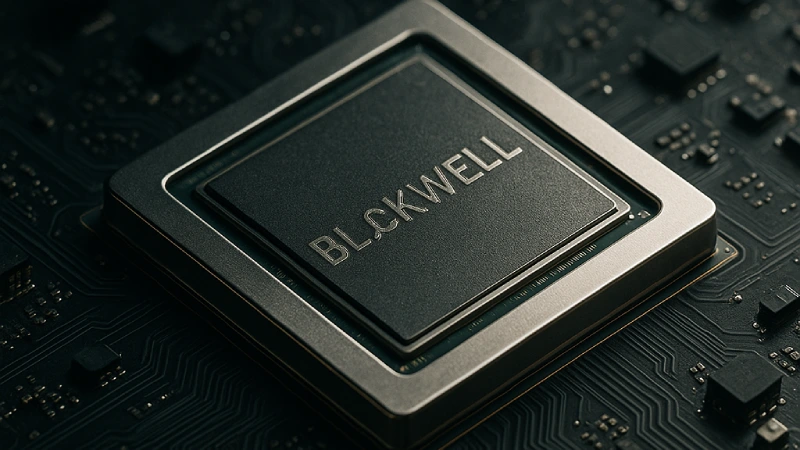
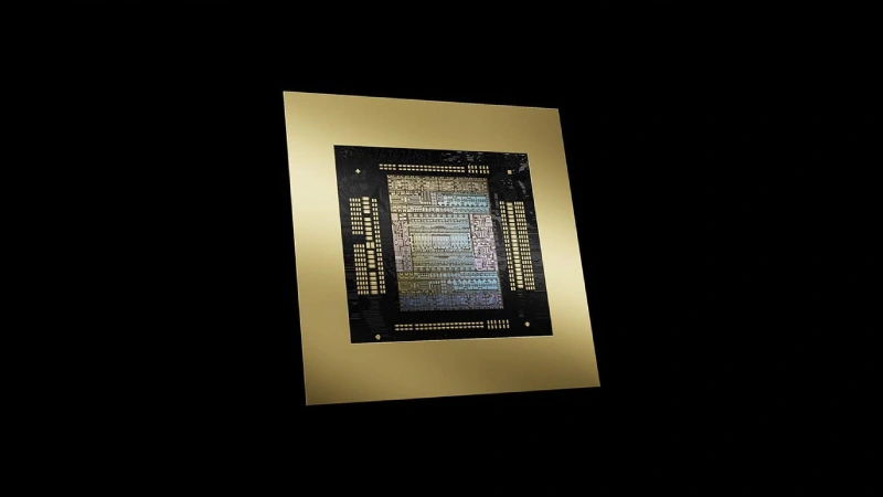
At the heart of the Blackwell architecture is the new NVIDIA Blackwell chip. At the core of the Blackwell architecture lies the new NVIDIA Blackwell chip. Being well capable, the processor packs 208 billion transistors, a huge count for one processor. This is a dramatic increase over the previous generation and is more than 2.5 times the transistors found on NVIDIA’s Hopper GPUs. The Blackwell chip is manufactured using a custom 4NP TSMC process.

A key innovation in the Blackwell design is its dual-die configuration. All NVIDIA Blackwell products feature two dies that are linked together. The sources provide slightly different figures for the speed of this chip-to-chip interconnect: one source states it is a 900GB/s link, while others mention a 10 TB/s interconnect. This interconnect provides the power of two GPUs within a single, fully cache-coherent, and full-stack-ready Blackwell chip. This design represents a significant leap from the single-chip designs of the Hopper generation.
Six Transformative Technologies
The NVIDIA Blackwell architecture is powered by six revolutionary new technologies built specifically for generative AI and accelerated computing. These innovations are expected to usher in leaps and bounds in various fields, including data science, electronic design automation (EDA), computer-aided engineering (CAE), and quantum computing. The five features are:

- Generative AI Engine/ Second-Generation Transformer Engine: This custom Tensor Core-based technology, along with innovations in NVIDIA TensorRT-LLM and NeMo frameworks, accelerates inference and training of LLMs, including very complex mixture of experts (MoE) models. New precision formats, including FP4 enablement and microscaling formats, enhance accuracy and throughput. It doubles the FP4 AI performance and supports expert parallelism methods with NVLink to train models of size 10 trillion-plus parameters.

- Confidential Computing: Blackwell infuses advanced confidential computing to protect AI models and customer data without any performance compromise. It supports various new native interface encryption protocols and significantly extends TEEs over to the GPU, becoming the first TEE-I/O-capable GPU. This holds huge significance in privacy-sensitive verticals such as healthcare and finance and is the protector of AI intellectual property. It achieves performance almost identical with unencrypted modes.
- 5th Generation on NVLink: To enhance and further boost the performance of multitrillion-parameter AI models and to allow smooth communication amidst scores of GPUs, the latest generation of NVLink takes the unprecedented leap of 1.8Tb/s (or 1.8TB/s) throughput per GPU, way beyond the bandwidth of PCIe Gen5. NVLink interconnects can scale up to 576 GPUs. The NVLink Switch Chip brings GPU bandwidth of 130TB/s within one 72-GPU NVLink domain (NVL72) and goes further to support clusters outside a single server, scaling GPU communications alongside increased computing.

- Decompression Engines: Dedicated decompression engines are included to support the latest formats and accelerate database queries. This innovation aims to deliver the highest performance in data analytics and data science. When combined with high-speed memory (HBM3e) and the Grace CPU interconnect (900GB/s), Blackwell is claimed to be 18X faster than CPUs and 6X faster than NVIDIA H100 GPUs in database operations.
- RAS Engine: Unique to Blackwell-powered GPUs is a dedicated engine for reliability, availability, and serviceability. This engine adds intelligent resiliency by monitoring hardware and software health using AI-driven predictive management to detect potential faults early on and prevent downtime. It provides in-depth diagnostic information to help identify areas of concern, plan maintenance, localize issue sources, and minimize downtime, maximizing system uptime and reducing operating costs for massive-scale AI deployments.

In addition to these specific engines and interconnects, the Blackwell architecture also features Multi-Instance GPU (MIG) capabilities, with 7 instances per GPU listed in the specifications table. It also includes decoders (2x 7 NVDEC, 2x 7 NVJPEG).
Performance and Use Cases
The NVIDIA Blackwell architecture is engineered to deliver unprecedented performance for a range of demanding workloads.
Generative AI and LLMs: Blackwell is purpose-built for this domain. It enables real-time inference on massive models scaling up to 10 trillion parameters. The GB200 NVL72, with its 30x inference speedup for trillion-parameter LLMs like GPT-MoE 1.8T, makes real-time performance possible for resource-intensive models. The architecture’s support for models up to 740 billion parameters in size (via HBM Model Size spec) also significantly exceeds previous capabilities.
The use of FP4 precision and advanced Tensor Core technologies is key to achieving this acceleration. Blackwell also accelerates AI model training, with the GB200 NVL72 providing 4x faster training speeds compared to Hopper GPUs for large models, leading to reduced rack space, TCO, and energy usage. The architecture’s ability to create detailed virtual realities can also accelerate the training of multimodal LLMs and robots.

Accelerated Computing and HPC: Blackwell is a cornerstone for breakthroughs in various accelerated computing fields. It enables high-speed performance for data processing, electronic design automation (EDA), and quantum computing. Blackwell enhances complex problem-solving in HPC applications that utilise numerical methods, simulations, and computations. While traditionally less GPU-dependent, the parallel computing power of Blackwell greatly accelerates HPC development, supporting hybrid configurations. Fields like physics, chemistry, geology, and biology benefit greatly from GPU-accelerated clusters for simulations and modelling.
Market Adoption and Availability
The Blackwell architecture and products were announced at the GTC 2024. NVIDIA expects tremendous interest and adoption from the leading tech companies such as Amazon Web Services (AWS), Dell Technologies, Google, Meta, Microsoft, OpenAI, Oracle, Tesla, and xAI, which will all reportedly use Blackwell in their AI and cloud computing offerings.
Neither pricing for the new GB200 chip nor that of the systems in which it will be used has yet been announced by NVIDIA. The last-generation H100 chip, which was the Hopper generation, was about $25,000 to $40,000. Specifically, the NVIDIA Blackwell GB200 NVL72/36 is expected to be available by the end of 2025, with early access reservations available through some providers. CUDO Compute has stated its intention to offer the NVIDIA B100 as soon as it is released and provides options to reserve access or upgrade from current H100/H200 instances.

NVIDIA faces competition in the AI chip market from rivals like Intel and AMD. Intel introduced AI chips like Gaudi3 and new processors with neural processing units last year, while AMD launched its MI300 data center GPU accelerator family. Gigabyte, a partner providing solutions for Blackwell, also offers server solutions featuring Intel Gaudi 3 and AMD Instinct MI300X. Despite this competition, NVIDIA holds a dominant position in the data center AI chip market, capturing roughly an 80% share last year.
Conclusion
The Blackwell architecture from NVIDIA represents a major turning point in the history of computing, owing to generative AI and HPC being two of its fast-growing fields. With its stitched-together and novel dual-die design constituting an unprecedented transistor count, along with a set of transformative technologies from the advanced Transformer Engine, Secure AI, high-speed NVLink, efficient Decompression Engines, and smart RAS Engine.
Blackwell shall be the platform in enabling the build-out and deployment of AI models at a scale never seen before. Performance and efficiency improvements were big, huge even, when put in comparison to the previous Hopper architecture, implying that cost-wise and energy-wise, workload-wise, the most expensive ones will now be cheaper to operate and consume less energy.

Products like the GB200 Grace Blackwell Superchip and the rack-scale GB200 NVL72 system demonstrate the architecture’s capability to accelerate AI inference, training, and data processing to new levels. As Jensen Huang stated, Blackwell is positioned as “a processor for the generative AI era”, serving as the “engine behind AI factories for the age of AI reasoning” and driving what he calls a “new industrial revolution”. With major industry players lining up to adopt Blackwell, its impact on the future of AI and accelerated computing is expected to be profound.
